Informations
The semiconductor world is rapidly changing, and this brings along challenges for Europe and all other leading semiconductor countries in the world. The mission of the European project INPACE is to identify the needs and opportunities for international collaboration in this changing ecosystem.
International cooperation is indeed key for speeding up technological innovation, reducing cost by avoiding duplicated research, strengthening complex semiconductor value chains, knowledge exchange, manage risks due to the turbulent geopolitical context, overcoming gaps in standardisation and skill shortage, and is encouraged by the new strategies of many semiconductor countries and is one of the objectives of the EU Chips Act 1 & 2.
The aim of this event is to strengthen bilateral cooperation between India and EU in important areas for future electronics systems and economic resilience, including technology challenges and possible solutions for advanced computing and advanced functionalities, value chains, manufacturing, industrial ecosystems, missing standards, and skill shortage.
The Semiconductors / Microelectronics sessions will focus in particular on the following topics of common interest between EU and India: Neuromorphic Computing, Power Devices, Sensing, Advanced Materials, Manufacturing and Upskilling.
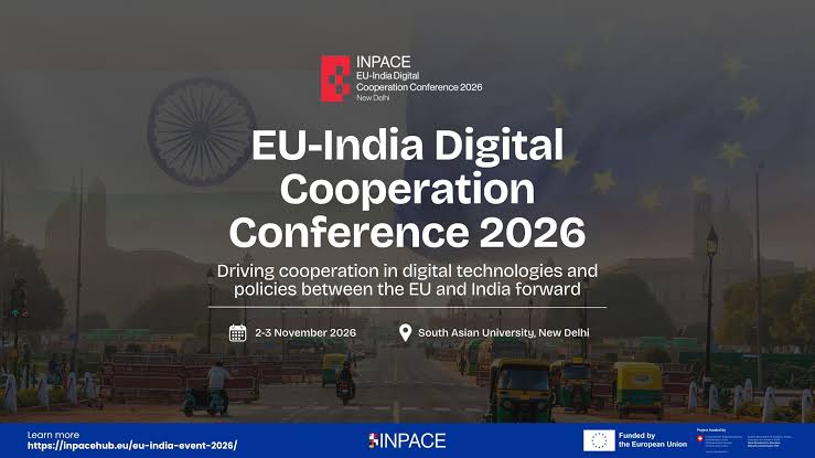
Semiconductor Workshop at the EU-India Digital Cooperation Conference 2026
Programme
Day1 – November 2nd, 2026
Manufacturing, Value Chain, Technologies & Skills
10:00 – 10:25
Francis Balestra SiNANO Institute / CNRS, France
Abstract:
The semiconductor world is rapidly changing, and this brings along challenges for Europe and all other leading semiconductor countries in the world. International cooperation is key for speeding up technological innovation, reducing cost by avoiding duplicated research, strengthening complex semiconductor value chains, knowledge exchange, manage risks due to the turbulent geopolitical context, and overcoming gaps in standardisation and skills. The aim of this presentation is to highlight the main challenges and need for cooperation between India and EU, covering the semiconductor industrial ecosystems, roadmaps, manufacturing, value chain, technologies for advanced computing and advanced functionalities, missing standards and skill shortage.
Bio:
Francis Balestra, CNRS Research Director at CROMA, is Director Emeritus of the European SINANO Institute and President of IEEE Electron Device Society France, and has been Director of several Research labs. He coordinated several European Projects (NEREID, NANOFUNCTION, NANOSIL, etc.) that have represented unprecedented collaborations in Europe in the field of Nanoelectronics, and is currently coordinator
of the Horizon Europe ICOS project dedicated to International Cooperation on Semiconductors with leading semiconductor countries.
He founded and organized many international Conferences, and has co-authored more than 500 publications. He is member of several European Scientific Councils, of the Advisory Committees of International Journals and of the IRDS (International Roadmap for Devices and Systems) International Roadmap Committee, as representative of Europe.
Chips2systems (C2S)
10:25 – 10:50
Vivian D. C-DAC, India
Importance of Workforce Development & Heterogeneous Integration Technology for India’s Semiconductor Industry
10:50 – 11:15
Shankara Prasad Indian Institute of Technology Guwahati, India
Abstract:
India has finally realized the importance of Semiconductor Technology for its economy as well as for social development. However, India’s focus on providing Design services to MNCs has to change. India also needs to recognize that technology development and establishing sub-nano Wafer Fabs is beyond its capability in the near future. Therefore, this talk will focus on how and why India should emphasise Heterogeneous Integration of micro-electronics, MEMS, and Photonics and related Advanced Packaging. And how to develop a workforce to meet this multi-domain technology development and manufacturing capability.
Bio:
Dr. Sayani Majumdar is an Associate Professor of Electrical Engineering at the Faculty of Information Technologies and Communication Sciences at Tampere University, Finland. She is also a visiting professor at the Miin Wu School of Computing at National Cheng Kung University, Taiwan. Her career in semiconductor device research spans more than two decades where she worked in both academia and in close collaboration with the industry. She worked on several emerging technologies in world-leading organizations including MIT, USA and Max-Planck Institute, Germany. Her team’s current research focuses on the development of embedded non-volatile memories and neuromorphic computing hardware using low-thermal budget ferroelectric and semiconductor materials and processes for their back-end-of-line integration with CMOS circuits for low-power neuromorphic edge devices and in cryogenic electronics for quantum and space applications.
Wide Band Gap devices for power applications
11:15 – 11:40
Enrico Sangiorgi University of Bologna, Italy
Abstract:
Wide-bandgap power devices are enabling major advances in power electronics through higher efficiency, faster switching, and increased power density compared with conventional silicon technologies. This talk will provide an overview of the current status of SiC and GaN power devices, highlighting their key characteristics, technological maturity, and main application areas. Attention will be devoted to some of the reliability challenges that may affect the widespread adoption of WBG technologies, as well as to selected approaches being investigated to improve device robustness and reliability. In the second part of the talk, the Italian National Research Center “Fondazione Chips-IT” will be presented.
Bio:
Enrico Sangiorgi is professor of Electronics at the University of Bologna and Director Emeritus of the Sinano Institute. He is a member of the Chips JU Governing Board and of the Foundation Chips-IT Supervisory Board.
He has been the first Director of Consorzio Nazionale Interuniversitario per la Nanoeletronica – IU.NET and Vice Rector for Teaching and Education at the University of Bologna.
Enrico Sangiorgi has been Editor of IEEE Electron Device Letters and Editor-in-Chief of the Journal of the Electron Device Society.
His research covers the physics, characterization, modeling, and fabrication of solid-state devices and integrated circuits, working on several aspects of device scaling, as well as device reliability for silicon and WBG devices.
Enrico Sangiorgi has coauthored more than 280 papers in major journals and conference proceedings. His publications received more than 5000 citations attaining a h-index of 35.
Enrico Sangiorgi is Distinguished Lecturer and Fellow of the IEEE.
Physics-based SPICE modeling framework for e-Mode power GaN technology facilitating automotive and data-center power electronics
11:40 – 12:05
Sheikh Aamir Ahsan National Institute of Technology Srinagar, India
Abstract :
The p-GaN gate HEMT technology is reshaping the landscape of automotive power electronics by enabling high-efficiency, high-frequency, and compact converter designs. This presentation introduces a physics-based, SPICE-compatible compact model for p-GaN gate AlGaN/GaN HEMTs, developed to bridge device-level physics with circuit-level simulation for automotive applications. Model electrostatics and transport formalism is presented, followed by modeling dynamic Rds-on by accounting for trapping and detrapping effects through mobility modulation, enabling accurate prediction of transient resistance variations under high drain voltage stress. Furthermore, we showcase the model’s capability to capture temperature-dependent gate leakage at different bias conditions. Subsequently, model results for the p-channel GaN counterpart are demonstrated, and deployed into GaN complementary circuits such as inverters, oscillators, comparators etc, and correlated with experimental results. Towards the end of the presentation, the model parameters are extracted from TCAD simulations and validated against mixed-mode boost converter results as well as from experimental results, demonstrating strong correlation in transient and steady-state behavior. The framework is then extended to system-level studies, deployed within a perturb-and-observe maximum power point tracking (MPPT) algorithm for photovoltaic sources and constant-current/constant-voltage (CC-CV) battery charging for electric vehicles. Lastly, demonstration of the LTspice / Qspice compatible model is carried out for a p-GaN monolithic bidirectional switch, with experimental validation against AC chopping. This versatile framework bridges device physics and circuit implementation for next-generation GaN-based power electronics.
Bio:
Sheikh Aamir Ahsan possesses expertise in state-of-the-art RF and power GaN SPICE models and simulation. Originating from the development of the ASM GaN model during his doctoral studies at IIT Kanpur, his team at NITSRI leads the advancement of power and RF GaN technology through modeling and design enablement frameworks. Acting as a consultant for diverse industrial entities, his GaN research seamlessly integrates into commercial SPICE simulators, influencing the trajectory of GaN product development and application globally. He also has a keen interest in 2D material FET model development – aiming for sensing, memory and neuromorphic applications. He was awarded the Startup Research Grant in 2019 by the Science and Engineering Research Board, and presently leads the ANRF PAIR-B with NITSRI as one of the spoke institutions, and is also one of the principal nvestigators for the forthcoming MAHA-2D mission project funded by ANRF and MEITY, Govt. of India.
2D Materials for resistive memories: simulations and perspectives
12:05 – 12:30
Alessandro Cresti CNRS, France
Abstract:
Their tunable electronic properties, atomic thinness, and mechanical flexibility, make 2D materials promising for developing sustainable devices. Nonvolatile memories, in particular, are emerging as versatile components with applications ranging from RF switches to neuromorphic computing. Among them are the atomristors, a few-layer 2D materials sandwiched between metallic contacts.
After an overview, I will present some simulations of pristine and defective atomristors to explore the role of different metallic contacts and 2D materials.
Our ongoing research, for which collaborations are welcome, extends these simulations to fully 2D ferromagnetic and ferroelectric memories, which could open new avenues for ultra-low-power, multifunctional electronics.
Bio:
Alessandro Cresti is a researcher at the French National Center for Scientific Research (CNRS), where he leads cutting-edge research in quantum transport simulations and emerging electronic technologies. He received his Ph.D. in physics from the University of Pisa in 2006 and has 20 years of experience studying the theory and computation of nanoscale electronic devices, particularly 2D materials such as graphene and transition metal dichalcogenides.
He develops advanced full-quantum simulation tools to explore the fundamental and applied aspects of electronic transport in nanostructures. He investigates innovative materials and device architectures for next-generation memory and logic applications, bridging the gap between theoretical insights and experimental advancements.
He also served as the scientific coordinator of the book Beyond-CMOS: State of the Art and Trends, a comprehensive reference on the physics and future prospects of emerging electronic technologies.
Day 2 – November 3rd, 2026
Neuromorphic Computing
09:30 – 9:55
Sreetosh Goswami, Indian Institute of Science, India
Abstract:
Artificial Intelligence (AI) has long been a subject of fascination, oscillating between grand promises and inevitable disillusionment. While remarkable milestones, like AI outperforming human champions in complex games, suggest we are entering a new era of computing, a deeper look reveals that these breakthroughs come at a steep cost — demanding vast amounts of energy and intensive, expensive training process. In areas like cognition, decision-making, and intelligence, even our most advanced computing machines fall far short of the brain’s unparalleled efficiency and compact design. The core of this challenge lies in the limitations of conventional circuit elements and computing architectures, which struggle to replicate the brain’s complex, nonlinear dynamics operating at the edge of chaos. In this seminar, I will introduce a new class of molecular circuit elements designed to capture the intricate, reconfigurable logic that mimics brain-like behaviour at the nanoscale. These devices can be operated as analog or digital elements, or could be poised on the verge of instability, offering a unique potential to emulate neural functions in ways that traditional computing hardware cannot. Our journey explores these molecular systems from their foundational physics and chemistry, all the way to integrated circuit design and on-chip applications [1-9] with the aim of laying the groundwork for AI and machine learning platforms that can transcend the limitations of Moore’s Law and lead to a new era of energy-efficient computing.
References:
[1] Sharma, D., Rath, S.P., Kundu, B., Korkmaz, A., Thompson, D., Bhat, N., Goswami, S., Williams, R.S. and Goswami, S. Linear symmetric self-selecting 14-bit kinetic molecular memristors. Nature 633, 560–566 (2024).
[2] Sreebrata Goswami, Williams, R. Stanley, and Sreetosh Goswami. “Potential and challenges of computing with molecular materials.” Nature Materials (2024): 1-11.
[3] Pallavi Gaur, Bidyabhusan Kundu, Pradip Ghosh, Shayon Bhattacharya, Lohit T, Harivignesh S, Santi P. Rath, Damien Thompson, Sreebrata Goswami and Sreetosh Goswami, Molecularly Engineered Memristors for Reconfigurable Neuromorphic Computing. Advanced Materials (2025): e09143.
[4] Goswami, S. Reflections on the past decade of neuromorphic computing. Nature Reviews Materials 11, 431–432 (2026).
[5] S, H., Bhat, N. & Goswami, S. Neuromorphic pathways for transforming AI hardware. Nature Electronics 8, 752–756 (2025).
Bio:
Sreetosh Goswami is Associate Professor at the Centre for Nanoscience and Engineering (CeNSE), Indian Institute of Science. He joined IISc in 2021 after receiving his Ph.D. from the National University of Singapore. His graduate research was recognised with gold medals at MRS Spring (Phoenix, 2018) and E-MRS (Warsaw, 2018), and the Best Contribution Award at Memrisys (Dresden, 2018). His group develops energy-efficient molecular neuromorphic hardware for AI, with applications in deep learning, signal and image processing, and bioinformatics. The broader aim is to move computing beyond conventional CMOS limits and to provide tools useful to the wider scientific community.
His recent recognitions include the Advanced Materials Rising Star (2025), iCANX Young Scientist Award (2025), Wiley Young Investigator Award (2025), INSA Young Associate (2025), IISc Research Award (2025), Young Associate of the Indian Academy of Sciences (2024), the Young Physicist Award (2024), MRS-S Young Scientist Medal (2023), and the Pratiksha Trust Young Investigator Chair (2021).
Ferroelectric-Material-Based Heterostructures as a Platform for Next-Generation Computing
9:55 – 10:20
Sayani Majumdar Tampere University, Finland
Abstract:
The explosive growth of Artificial Intelligence (AI) is pushing today’s computing infrastructure to its limits. Exponentially rising demands for computation and electrical power are rapidly becoming unsustainable, exposing the urgent need for radically new hardware, systems that are not only more scalable and compact, but dramatically more energy efficient. Neuromorphic computing, inspired by the event-driven, massively parallel architecture of the human brain, offers a transformative path forward. With emerging device technologies enabling true in-memory computation and tightly integrated sensing, we are heading towards capabilities far beyond conventional CMOS. Yet achieving brain-level processing complexity in silicon will require breakthroughs in advanced materials. Beyond neuromorphic systems, scalable quantum computing, space technologies, and electronics designed for extreme environments similarly depend on materials innovation to move forward. In this talk, I will present ferroelectric-material-based heterostructures as a powerful platform for next generation computing hardware, focusing on CMOS back-end compatible Fluorite ferroelectric Hf0.5Zr0.5O2 (HZO) over a broad temperature range of 4 – 400 K. I will discuss how their unique material properties and device physics unlock new possibilities, from dense embedded memory and optoelectronic data conversion to cryogenic data storage and in-memory computing. When integrated with back-end processable semiconductors like 2D materials and Indium-Gallium-Zin-Oxide (IGZO), ferroelectric devices with ultralow off current offer decisive advantages for neuromorphic computing, integrated sensing, photonic-to-electrical conversion, and energy-efficient operation under demanding conditions. However, realizing their full potential requires a deep understanding of their scalability, reliability, yield, and fault tolerance, particularly as these emerging devices integrate with advanced node CMOS and operate under harsh conditions. By properly designing and engineering of these materials and their interfaces, we can define a new trajectory for computing hardware, one capable of bringing powerful AI to resource-constrained edge platforms, upscaling quantum computing or making autonomous intelligent systems possible under harsh environments like space.
Bio:
Dr. Sayani Majumdar is an Associate Professor of Electrical Engineering at the Faculty of Information Technologies and Communication Sciences at Tampere University, Finland. She is also a visiting professor at the Miin Wu School of Computing at National Cheng Kung University, Taiwan. Her career in semiconductor device research spans more than two decades where she worked in both academia and in close collaboration with the industry. She worked on several emerging technologies in world-leading organizations including MIT, USA and Max-Planck Institute, Germany. Her team’s current research focuses on the development of embedded non-volatile memories and neuromorphic computing hardware using low-thermal budget ferroelectric and semiconductor materials and processes for their back-end-of-line integration with CMOS circuits for low-power neuromorphic edge devices and in cryogenic electronics for quantum and space applications.
Neuromorphic Computing using Spintronic Devices
10:20 – 10:45
Dr. Arshid Nisar National Institute of Technology Srinagar, India
Abstract: The growing demands of artificial intelligence are driving the need for energy- and hardware-efficient computing beyond conventional von Neumann architectures. Spintronic devices offer a promising platform for neuromorphic computing owing to their non-volatility, intrinsic dynamics, high endurance, and potential for low-energy operation. This talk will present recent advances in spintronic device-based neuromorphic computing, with a focus on emerging magnetic devices and their application to implement fundamental neuronal functions and synaptic weight storage. The discussion will also cover how these neurons and synapses can be combined to realize various artificial neural networks and in-memory computing architectures. Finally, the talk will discuss key challenges in realizing practical spintronic neuromorphic systems.
Smart Sensing
10:45 – 11:10
Alan O’Riordan Tyndall, Ireland
Abstract:
Smart Sensors
11:10 – 11:35
Shiv Govind Singh IIT Hyderabad, India
Abstract:
Closing Remarks – Francis Balestra SiNANO Institute/CNRS
11:35 – 11:45
Working Session – Collaboration opportunities on Semiconductors
14:15 – 15:30
Organiser Dr. Francis Balestra SiNANO Institute, France
Summary:
The Cluster 4 Working Session will be devoted to discussing possible topics and instruments for future EU-India cooperation. The Session will cover the fields of common interest in India and Europe, as well as the best collaboration tools, including joint R&D&I projects, exchanges of students and researchers, joint Masters and PhDs, international training activities and Summer Schools, student internship, joint roadmapping, organisation of in-person and virtual Workshops for knowledge exchange and matchmaking, access to Research Infrastructures, standardisation needs for emerging technologies, cooperation in the semiconductor value chain, Position papers for future joint activities, and possible European and Indian funding.


