Sinano Workshop 2006
The 2nd Sinano Workshop was held during the ESSDERC-ESSCIRC conference in Montreux, Switzerland on September 22th, 2006.
Programm of the Workshop
“New generation of SiGe virtual substrates ” – T. Grasby, Warwick University
“Strain characterisation in advanced Si devives ” – S. Olsen, Newcastle University
“Characterization of Nanoscale dielectrics ” – O. Engstrom, M. Lemme, P. Hurley, S. Hall, Chalmers Univ., AMO, Tyndall, Liverpool University
“Reliability degradation characteristics of ultra-thin gate dielectrics for Nano-CMOS application ” – J.F. Kang, N. Sa, B.G. Yan, J.F. Yang, X.Y. Liu, R.Q. Han, Y.Y. Wang, Beijing University
“Comparison among modelling approaches for gate current computation in advanced gate stacks ” – P. Palestri et al, University of Udine
“Comparison among modeling approaches for drain current computation in nanoMOSFETs ” – C. Fiegna et al, University of Bologna
“CMOS for next 15 years as the mainstream of nano device technology: problems, solutions and beyond that ” – H. Iwai, Tokyo Institute of Technology
“Emerging devices for enhancing and beyond the CMOS technology ” – W.-X. Ni, National Nanodevice Laboratories, Hsinchu
“Quantum transport in semi-conductor nanowire MOSFETs: influence of the bandstructure ” – M. Bescond, IMEP
“Silicon Nanodots and related structures for memory application ” – A.G. Nassiopoulou, A. Salonidou, O. Winkler, B. Spangenberg, H. Kurz, A. Souifi, V. Bayot, A. Nazarov, IMEL, RWTH, LPM-CNRS, UCL, SPI
“Ultimate CMOS-compatible tunneling devices ” – A. Zaslavsky, Brown University


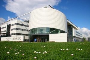
 Minatec – CROMA