In this space, we usually promote some job offers from the SiNANO members (PhD, internship, post-doc, position…).
Head of INL Technology Transfer Office (INL-TTO)
- INL was created with the aim of boosting Nanotechnology research and its impact in society, at a regional, Iberian and international level, starting by putting together a world class research infrastructure, attracting top principal investigators (PIs), creating new know-how and intellectual property, collaborating with existing companies as well as stimulating the creation of new spin-off start-ups. INL was conceived to assure world-class research excellence in all its activity areas and to:
- Develop partnerships with the industry and foster the transfer of knowledge into economic value and jobs;
- Train researchers and contribute to the development of a skilled workforce for the nanotechnology industry, through the implementation of joint training programs with universities and RTD centres;
- Attract international companies to the region;
- Boost the regional technology transfer system for local industry.
Candidates must have a track record in intellectual property protection, technology transfer, contracts and licensing experience demonstrated by agreements with the private sector. Experience in the electronics sector is desirable. A successful candidate must have the ability to lead a team with the charter of enhancing and expansion of our technology portfolio, thus successfully positioning INL as a leading innovating facility in nanotechnology. It is essential that the TTO head has decision-making that allows them to unblock crossroads that may be reached both with external entities, but also internally.
Details: here
Deadline application: January 27th, 2025, 23h00m (Lisbon Time)
- They are looking for a highly motivated postdoctoral researcher to work on the neuromorphic computing and sensing hardware development. This involves device design, fabrication and characterization as well as semiconductor process development in a state-of-the-art cleanroom facility. Materials synthesis will include atomic layer deposition (ALD), sputter and e-beam evaporation for metallic, semiconducting and dielectric oxides, and heterostructures based on these materials.
- The position will involve a combination of experimental and simulation work and requires close collaboration with doctoral students in the group, the Thin Film Electronics Laboratory led by Assoc. Professor Sayani Majumdar in Tampere University, Finland.
- Main topic of research will be on CMOS Back end compatible ferroelectric device development (Ferroelectric Capacitor, FeFET, Ferroelectric tunnel junctions, one of the most promising new memory technologies for neuromorphic hardware and will explore new material combinations and unique process technology to achieve device performance beyond the best available today.
Main duties include:
- High-level academic research and publication activities (90%)
- Teaching assistance in related graduate courses (10%)
- Please see also the detailed descriptions above
Details: here
Deadline application: 31/01/2025
- The position will be placed at the Division of Solid-State Electronics, Department of Electrical Engineering. It is planned for one year, with the possibility of prolongation for another year.
- Project description: The project aims to develop innovative neuromorphic transistors with inherent biological resemblance by utilizing 2D semiconductors and antiferroelectric films. The envisioned transistors will be used to construct compact and low-power neuromorphiccircuits. The research includes material preparation, device fabrication and circuit design. The research will be performed in a multidisciplinary environment therein scientists of complementary backgrounds collaborate
Duties:
- Preparation and characterization of ferroelectric/antiferroelectric film by ALD, e.g.
ZrO2, HfZrO2. - Design and fabrication of antiferroelectric-gating 2D-semiconductor field-effect
transistors. - Characterisation, optimization and modelling of the transistors.
- Design and demonstration of neuromorphic circuits using the transistors to emulate
the function of biological neurons.
Details: here
Deadline application: 9/02/2025
- 3PhD and one post-doc positions to work on advanced techniques for on-wafer characterization and modelling of SOI devices
The Louvain School of Engineering of Université catholique de Louvain (UCLouvain) is seeking for three RF Device Engineering PhD student (4 years) and one post-doc (3 years) to work on advanced techniques for on-wafer characterization and modelling of Silicon-on-Insulator (SOI) devices in a wide frequency and temperature ranges. You will also be expected to supervise master’s theses.
- The PhD students will be hosted by the RF-SOI Group of the Louvain School of Engineering. Under the guidance of Prof. J.-P. Raskin, the group has pioneered the widespread use of SOI for RF and microwave applications by establishing a clear path to transform lossy SOI substrates into quasi-lossless material. Thanks to those developments SOITEC’s eSI™ RF-SOI substrate has been able to displace III-V on the mobile handset RF switch market and at present almost all new smartphones have RF-SOI inside.
Details: here
Positions posted on 12/11
Apply with the support of the CROMA laboratory to the competitive entrance examinations for CNRS researcher permanent position.
Post-Doc position: Simulation and characterization of the influence of traps in the current fluctuations (LFN/RTN) of nanoscale FDSOI MOSFETs
In the framework of the IPCEI (Important Project of Common European Interest) and in collaboration with ST Microelectronics, we are working on the assessment of electrical noise phenomena in FDSOI MOSFETs, which are mainly related to oxide interface defects. In particular, a great focus is given in the study of Random Telegraph Noise (RTN), especially in its properties with regards to the shrinking of the channel length, which makes it challenging to predict or model. This type of noise can be detrimental for memory operation or CMOS imager performance.
We are offering :
• A 1-year (min.) full-time contract at a research laboratory internationally recognized for its
contribution in electrical characterization and noise studies, in the innovative city of Grenoble (France)
• A challenging topic with aspects of fundamental research and a simultaneously high industrial interest
• A combination of simulation and experimental work (all tools already available)
• A dynamic environment: 1 Research Associate and 1 Associate Professor supervising the work, 2 support engineers, 1 intern supporting the same topic and cutting-edge equipment for all necessary measurements and simulations
• The opportunity to work in close collaboration with a large industry like ST Microelectronics and potentially perform some additional measurements at ST Crolles
Details: here
Published on October 16/10/24.


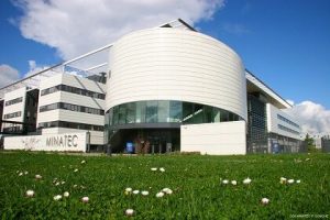
 Minatec – CROMA